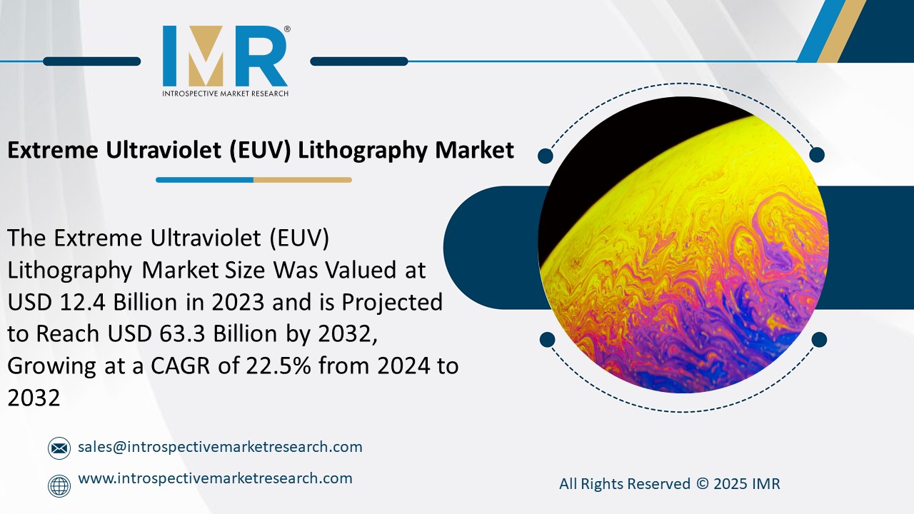
According to a new report published by Introspective Market Research, titled, Extreme Ultraviolet (EUV) Lithography Market by Type, Application, and End-Use Industry, The Global Extreme Ultraviolet (EUV) Lithography Market Size Was Valued at USD 12.4 Billion in 2023 and is Projected to Reach USD 63.3 Billion by 2032, Growing at a CAGR of 22.5% from 2024 to 2032 The global Extreme Ultraviolet (EUV) lithography market is witnessing unprecedented growth due to the increasing demand for advanced semiconductor manufacturing and miniaturized electronic devices. EUV lithography technology enables the fabrication of high-precision microchips at sub-10 nanometer scales, surpassing the limitations of traditional deep ultraviolet (DUV) lithography. This technology is critical for semiconductor foundries to enhance chip performance, power efficiency, and transistor density while maintaining production scalability.
EUV lithography offers a range of advantages over conventional lithography methods, including higher resolution, reduced processing steps, and improved yield rates. It is widely adopted in the production of processors, memory chips, and high-performance integrated circuits used in smartphones, data centers, automotive electronics, and AI applications.
The increasing trend of digitalization, AI deployment, and IoT devices is further driving demand for smaller, faster, and more efficient semiconductor devices. EUV lithography is instrumental in meeting these requirements, enabling chip manufacturers to produce next-generation nodes while reducing manufacturing complexity and operational costs. Strategic investments by major semiconductor companies are expected to further accelerate market growth over the forecast period.
The Extreme Ultraviolet (EUV) Lithography Market is segmented into Type, Application, and End-Use Industry. By Type: (High-NA EUV, Standard EUV) By Application: (Semiconductor Manufacturing, MEMS, Photonics, Others) By End-Use Industry: (Consumer Electronics, Automotive, Data Centers, Industrial Electronics, Healthcare, Others)
A key growth driver of the EUV lithography market is the growing demand for advanced semiconductor devices driven by AI, 5G, and IoT technologies. These applications require highly miniaturized and high-performance chips, which traditional DUV lithography cannot efficiently produce. EUV lithography enables higher-resolution patterning at smaller nodes, improving transistor density and reducing chip power consumption. Semiconductor foundries and integrated device manufacturers are increasingly investing in EUV tools to accelerate the production of advanced microchips, thereby driving widespread adoption of this cutting-edge technology.
A major market opportunity lies in High-NA EUV lithography systems, which provide enhanced resolution for next-generation semiconductor nodes below 3 nm. High-NA systems enable chipmakers to produce smaller, faster, and more energy-efficient processors and memory chips. Companies developing or integrating High-NA EUV technology can capitalize on the rising demand for advanced microchips in AI, cloud computing, automotive, and mobile applications. This presents an opportunity to capture premium market segments while addressing the semiconductor industry's evolving needs for precision, yield optimization, and manufacturing efficiency.
Extreme Ultraviolet (EUV) Lithography Market, Segmentation
The Extreme Ultraviolet (EUV) Lithography Market is segmented on the basis of Type, Application, and End-Use Industry.
Type
The Type segment is further classified into High-NA EUV and Standard EUV. Among these, the Standard EUV sub-segment accounted for the highest market share in 2023. Standard EUV tools are widely adopted in semiconductor fabs due to their established performance, availability, and ability to meet current production needs. They are critical for producing 7 nm and 5 nm node devices, allowing chipmakers to maintain high throughput and yield while preparing for the transition to High-NA EUV systems.
Application
The Application segment is further classified into Semiconductor Manufacturing, MEMS, Photonics, and Others. Among these, the Semiconductor Manufacturing sub-segment accounted for the highest market share in 2023. EUV lithography plays a central role in producing high-density, advanced semiconductor chips for consumer electronics, AI, and data center applications. Its ability to achieve ultra-fine patterning reduces processing steps, improves efficiency, and enables next-generation chip designs, making it indispensable for leading semiconductor manufacturers globally.
Some of The Leading/Active Market Players Are-
- ASML Holding N.V. (Netherlands)
- Canon Inc. (Japan)
- Nikon Corporation (Japan)
- Tokyo Electron Limited (Japan)
- Applied Materials, Inc. (United States)
- KLA Corporation (United States)
- Lam Research Corporation (United States)
- Hitachi High-Tech Corporation (Japan)
- Veeco Instruments Inc. (United States)
- Ultratech (United States)
- Veeco Instruments Inc. (United States)
- Gigaphoton Inc. (Japan)
- other active players.
Key Industry Developments
-
In February 2024, ASML launched its next-generation High-NA EUV lithography system.
The system provides superior resolution for sub-3 nm nodes, enabling chipmakers to produce highly dense and energy-efficient processors. This launch strengthens ASML’s technological leadership and addresses growing industry demands for advanced lithography tools, essential for AI, cloud computing, and automotive semiconductor production. - In July 2024, Nikon Corporation announced a strategic collaboration with a leading semiconductor fab to implement EUV lithography in high-volume production.
The partnership aims to accelerate mass production of 5 nm and below chips while optimizing yield and throughput. It highlights Nikon’s focus on expanding its EUV portfolio and supporting the global semiconductor industry's transition to next-generation nodes.
Key Findings of the Study
- Standard EUV dominates due to established performance and adoption.
- Semiconductor manufacturing is the largest application segment, driven by demand for advanced chips.
- High-NA EUV presents significant growth opportunities for next-generation nodes.
- North America and Asia-Pacific are leading regions due to semiconductor fab concentration.
- Technological innovation, strategic partnerships, and AI/IoT adoption drive market expansion.