
Semiconductor Manufacturing Equipment Market Demand Outlook, Regional Trends & Forecast (2024-2035)
Electronics and SemiconductorsPublished On : Mar 2026

Silicon On Insulator (SOI) Market Size By Product (Mems Devices, Optical Communication, RF Fem Products, Power Products, And Image Sensing), Technology (Smart Cut, Bonding SOI, And Layer Transfer SOI), Wafer Type (FD-SOI {Fully Depleted Silicon On Insulator}, PD-SOI {Partially Depleted Silicon On Insulator}, POWER-SOI, RF-SOI, And Emerging-Soi), Wafer Size (200 Mm, And 300 Mm), Application, Region- Global Market Analysis And Forecast, 2024-2032


Silicon on Insulator (SOI) Market Size Was Valued at USD 1.9 Billion In 2023 And Is Projected to Reach USD 5.89 Billion By 2032, Growing at A CAGR of 13.4% From 2024-2032.
In semiconductor manufacturing silicon on insulator (SOI) technology is the fabrication of the silicon semiconductor devices in layered silicon???insulator???silicon substrate, to overcome exploitative capacity within the device, thereby enhancing performance. SOI-based devices are different from conventional silicon-built devices in that the silicon junction is above an electrical insulator, generally silicon dioxide or sapphire (these types of devices are known as silicon on sapphire or SOS). The choice of insulator depends largely on intended utilization, with sapphire being applied for high-performance radio frequency (RF) and radiation-sensitive applications, and silicon dioxide for diminished short-channel effects in other microelectronics devices. The insulating layer and topmost silicon layer also vary extensively with the application.
In addition, silicon is one of the most used semiconductor materials. It is typically simple to change into a pure single crystal. Not at all like some other semiconductor materials, is silicon firm when heated at high temperatures. The great chemical and electrical properties of thermally designed SiO2 are presumably the highly beneficial factor that has made silicon such an effective semiconductor material. Silicon on Insulator (SOI) serves the demand of the electronic industry and hence the market of Silicon on Insulator (SOI) will rise and build with the varied demands in the electronics domain. The electronic reverberation in the industry has caused a surge in consumer electronics such as digital television, gaming consoles, cameras, kitchen appliances, and others. Furthermore, an increase in demand for high performance, low power, and low area among microelectronic devices accelerates the silicon on insulator market growth during the forecast period.

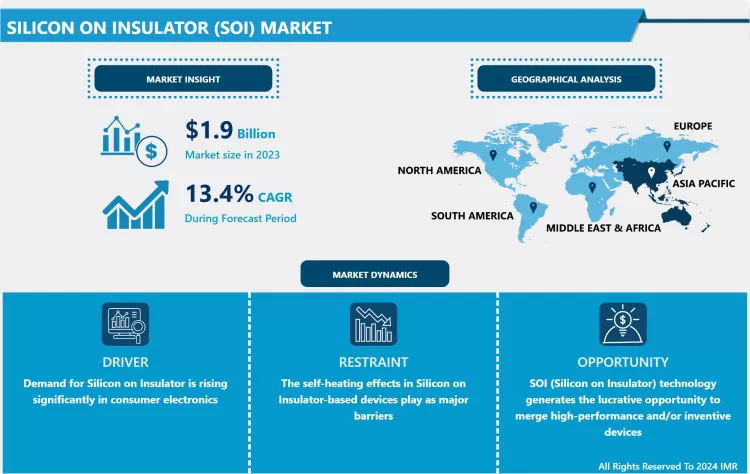
Silicon on insulator (SOI) is an essential part of consumer electronics products such as smartphones, wearable devices, tablets, electric cars, and others. Therefore, demand for Silicon on Insulator is rising significantly in consumer electronics. In addition, major requirements for the decreasing power utilization in a variety of mobile and portable devices have stimulated the demand for Silicon on Insulator devices in the consumer electronics industry. Moreover, the Silicon on Insulator wafers provides reliability, speed, and hardness beyond traditional technologies, which raises the overall operational performance at low voltage, which is further anticipated to add to the silicon on insulators market growth over the forecast period. Silicon on insulators catches a lot of attention in the development of high-performance circuits. In recent times, chipmakers giants such as IBM, Intel Corporation, and Advanced Micro Devices, have taken a surging interest in the commercialization of Silicon on Insulator technology. The minor reorganization in the current chip fabrication methods has allowed different manufactures to shift from the bulk silicon technology to Silicon on Insulator-based devices. The application of SOI has led to an exponential broadening of communication bandwidth and therefore is being employed in satellite communication and direct-link entertainment. Furthermore, aerospace and military are other scopes owing to the various requirements which lead to the growth of the market during the forecast period.
The self-heating effects in Silicon on Insulator-based devices play as major barriers to the growth of the silicon on insulator market. In addition, although a Silicon on Insulator wafer has various significances, it still is not preferred for utilization in different applications. The main reason is the declined breakdown voltage, floating body, and self-heating effects in Silicon on Insulator wafer-based devices. Decreased breakdown voltage levels severely limit the maximum supply voltage at which Silicon on Insulator wafer based-circuits and devices can operate. When the parasitic device turns on, the Silicon on Insulator wafer-based transistor cannot be switched off by switching the gate bias.
SOI (Silicon on Insulator) technology generates the lucrative opportunity to merge high-performance and/or inventive devices which can push away the present frontiers of the CMOS downscaling. Silicon on Insulator appears as the final relay of the Si-based microelectronics. The short-term prospects of Silicon on Insulator depend on the perforation rate of SOI circuits into the market. Not only does SOI provides improved performance, but also most of Silicon on Insulator barriers (self-heating, hot-carriers, early breakdown, etc.) disappear for operation at low voltage.
Based on the product, the MEMS device segment is expected to dominate the Silicon on Insulator (SOI) market during the forecast period. SOI is an extensively versatile starting material for fabricating micromechanical systems both with and without the incorporation of silicon integrated circuits on a shared substrate. The SOI technology allows customizing mechanical properties in addition to electrical properties in a very authentic way. This basic process point offers a basic significance to the use of SOI starting material in MEMS applications. MEMS structures also have high aspect ratios and highly complex 3D shapes resulting from anisotropic wet etching and wafer bonding. These generate novel requirements for successive lithography, doping, and thin-film processes.
Based on the technology, smart cut technology is expected to register the maximum Silicon on Insulator (SOI) market share over the forecast period. Smart cut technology provides a different significance, such as good homogeneity in thickness and the high quality of the transferred layer. In addition, the remainder of the first wafer may be reused as a new first or second wafer. Furthermore, it is a very generic and adaptable process owing to utilized to gain an extensive variety of single-crystal layers on top of many different supports.
Based on the wafer type, (FD-SOI) Fully Depleted Silicon on Insulator segment is expected to hold the largest Silicon on Insulator (SOI) market share throughout the forecast period. FD-SOI uses an ultra-thin layer of silicon over a buried oxide as a means to overcome leakage and variation in chips. FDSOI also boasts a back-bias feature. The most captivating market for FD-SOI resides at the 28nm node. 28nm is expected to be a long-running node. But the bulk CMOS camp won't give up the 28nm market so easily. TSMC, for instance, recently diversified its process lineup with the latest and cheap 28nm bulk CMOS derivative.
Based on the wafer size, the 300mm wafer size segment is anticipated to dominate the Silicon on Insulator (SOI) market over the forecast period. The increase and surface preparation of bulk SOI wafers has been boosted across the years. It is now possible to obtain very high-quality wafers in large diameters such as 300 mm. In addition, over the past few years, there has been a huge growth in the application of 300 mm wafers. FD-SOI wafers, the latest addition to the SOI wafer type segment, are built with 300 mm wafers.
Based on the application, the Photonics segment is expected to dominate the market during the forecast period. SOI discovers its extensive application in sensors for satellites owing to its supports in the computation of accurate readings and has sturdy operation capabilities. The development of Photo Voltaic technology and rising investment by economies to overcome carbon footprint will further raise the SOI market. In addition, SOI wafers are highly utilized in silicon photonics. The crystalline silicon layer on the insulator can be used to fabricate optical waveguides and other optical devices, either passive or active (for instance, by suitable implantations). The buried insulator allows the propagation of infrared light in the silicon layer based on total internal reflection. The top surface of the waveguides can be either left uncovered and revealed to air (For instance, for sensing applications), or covered with a cladding, typically made of silica. There is still a scope of development in terms of radiation resistance and thermal capacity for SOI.
Asia-Pacific region is expected to record the maximum market growth during the forecast period due to the emerging integrated circuit industry. India, South Korea, China, and Taiwan are estimated to register for a significant market share in the region, owing to growing industrial application, economic developments, and technology adoption for different industrial operations. In addition, a few of the major drivers for the growth of the SOI market in the region include the eminence of the semiconductors industry in the region. The presence of key chip producers and foundry players in APAC is anticipated to lead to increased demand for SOI wafers in the region, therefore contributing to the growth of the Silicon on Insulator market in the region.
North America region is expected to witness significant market growth for the Silicon on Insulator. Growing demand for computing, gaming consoles, microprocessors, and mobile applications are the major factors for the growth of silicon on the insulator market in the region. In addition, being the presence of major key players such as GLOBAL FOUNDERS, IBM, and others in the region is expected to hasten the growth of the Silicon on Insulator market over the forecast period.
|
Silicon on Insulator (SOI) Market |
|||
|
Base Year: |
2023 |
Forecast Period: |
2024-2032 |
|
Historical Data: |
2017 to 2023 |
Market Size in 2023: |
USD 1.9 Billion |
|
Forecast Period 2024-32 CAGR: |
13.4% |
Market Size in 2032: |
USD 5.89 Billion |
|
Segments Covered: |
By Type |
|
|
|
By Technology |
|
||
|
By Wafer Type |
|
||
|
By Wafer Size |
|
||
|
By Application |
|
||
|
By Region |
|
||
|
Key Market Drivers: |
|
||
|
Key Market Restraints: |
|
||
|
Key Opportunities: |
|
||
|
Companies Covered in the report: |
|
||
|
Silicon on Insulator (SOI) Market |
|||
|
Base Year: |
2023 |
Forecast Period: |
2024-2032 |
|
Historical Data: |
2017 to 2023 |
Market Size in 2023: |
USD 1.9 Billion |
|
Forecast Period 2024-32 CAGR: |
13.4% |
Market Size in 2032: |
USD 5.89 Billion |
|
Segments Covered: |
By Type |
|
|
|
By Technology |
|
||
|
By Wafer Type |
|
||
|
By Wafer Size |
|
||
|
By Application |
|
||
|
By Region |
|
||
|
Key Market Drivers: |
|
||
|
Key Market Restraints: |
|
||
|
Key Opportunities: |
|
||
|
Companies Covered in the report: |
|
||
The forecast period in the market research report is 2024-2032.
Silicon on Insulator (SOI) Market Size Was Valued at USD 1.9 Billion In 2023 And Is Projected to Reach USD 5.89 Billion By 2032, Growing at A CAGR of 13.4% From 2024-2032.
Related Reports
Understand your customers' needs so can deliver better services and experiences.
Stay in touch with us to get latest news and discount coupons.